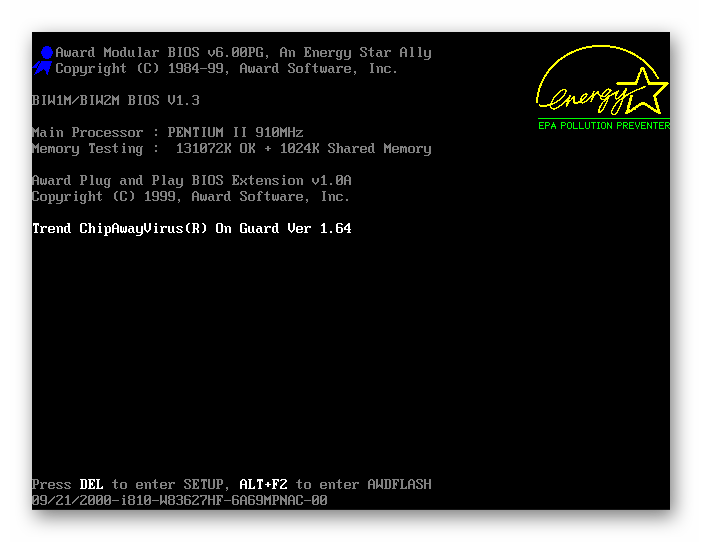
bios signals. sound short and long beeps when turning on the PC
The BIOS is responsible for checking the functionality of the main components of the computer before each power-up. Before the OS is loaded, BIOS algorithms check the hardware for critical errors. If any are found, then instead of loading the operating system, the user will receive a series of certain sound signals and, in some cases, display information on the screen.
BIOS is actively developed and improved by three companies - AMI, Award and Phoenix. Most computers have built-in BIOS from these developers. Depending on the manufacturer, sound alerts may vary, which is sometimes not very convenient. Let's take a look at all the computer's turn-on signals from each developer.
AMI beeps
With this developer, sound alerts are distributed by beeps - short and long signals.

Sound messages are given without pauses and have the following meanings:
- The absence of a signal means a malfunction of the power supply or the computer is not connected to the network;
- 1 short signal - accompanied by the start of the system and means that no problems were detected;
- 2 and 3 short messages are responsible for certain malfunctions with RAM. 2 signal - parity error, 3 - the inability to start the first 64 KB of RAM;
- 2 short and 2 long signal - malfunction of the floppy disk controller;
- 1 long and 2 short or 1 short and 2 long- video adapter failure. Differences may be due to different BIOS versions;
- 4 short signals indicate violations of the system timer. It is noteworthy that in this case the computer may start, but the time and date in it will be knocked down;
- 5 short messages indicate CPU inoperability;
- 6 short signals indicate a problem with the keyboard controller. However, in this case, the computer will start, but the keyboard will not work;
- 7 short messages - a malfunction of the system board;
- 8 short beeps indicate an error in the video memory;
- 9 short signals is a fatal error when starting the BIOS itself. Sometimes restarting the computer and / or resetting BIOS settings helps to get rid of this problem;
- 10 short messages indicate an error in the CMOS memory. This type of memory is responsible for correctly saving the BIOS settings and starting it when turned on;
- 11 short beeps in a row means that there is a serious problem with the cache memory.
Audible Signals Award
Sound alerts in the BIOS from this developer are somewhat similar to signals from the previous manufacturer. However, Award has fewer of them.
Let's decipher each of them:
- The absence of any sound alerts may indicate problems with the connection to the mains or problems with the power supply;
- 1 short a non-repeating signal is accompanied by a successful launch of the operating system;
- 1 long the signal indicates problems with RAM. This message can be played either once or repeated for a certain period of time, depending on the motherboard model and BIOS version;
- 1 short the signal indicates problems with the power supply or a short circuit in the power transmission circuit. It will go continuously or repeat at a certain interval;
- 1 long and 2 short alerts indicate the absence of a graphics adapter or the inability to use video memory;
- 1 long signal and 3 short warn about a malfunction of the video adapter;
- 2 short signals without pauses indicate small errors that occurred during startup. Data on these errors is displayed on the monitor, so you can easily deal with their solution. To continue loading the OS, you will have to click on F1 or Delete, more detailed instructions will be displayed on the screen;
- 1 long message and subsequent 9 short indicate a malfunction and / or failure to read BIOS chips;
- 3 long signals indicate a problem with the keyboard controller. However, the operating system will continue to load.
Phoenix beeps
This developer has made a large number of different combinations of BIOS signals. Sometimes this variety of messages causes problems for many users to identify the error.
In addition, the messages themselves are quite confusing, as they consist of certain sound combinations of different sequences. The decoding of these signals is as follows:
- 4 short—2 short—2 short messages mean the completion of component testing. After these signals, the operating system will start loading;
- 2 short—3 short—1 short a message (the combination is repeated twice) indicates errors in the processing of unexpected interrupts;
- 2 short—1 short—2 short—3 short a signal after a pause indicates an error when checking the BIOS for copyright compliance. This error is more common after updating the BIOS or when you first start the computer;
- 1 short—3 short—4 short—1 short the signal reports an error that was made when checking the RAM;
- 1 short—3 short—1 short—3 short messages occur when there is a problem with the keyboard controller, but the operating system will continue to load;
- 1 short—2 short—2 short—3 short beeps warn of an error in the calculation of the checksum when starting the BIOS .;
- 1 short and 2 long beeps indicate an error in the operation of adapters that can have their own BIOS built into them;
- 4 short—4 short—3 short you will hear a beep when there is an error in the math coprocessor;
- 4 short—4 short—2 long a signal will report an error in the parallel port;
- 4 short—3 short—4 short signals indicate a failure of the real time clock. With this failure, you will be able to use the computer without any difficulty;
- 4 short—3 short—1 short the signal indicates a problem with the RAM test;
- 4 short—2 short—1 short the message warns of a fatal failure in the central processor;
- 3 short—4 short—2 short you will hear if there are any problems with the video memory or the system cannot find it;
- 1 short—2 short—2 short beeps indicate a failure in reading data from the DMA controller;
- 1 short—1 short—3 short beeps will sound when an error is associated with the operation of CMOS;
- 1 short—2 short—1 short a beep indicates a problem with the system board.
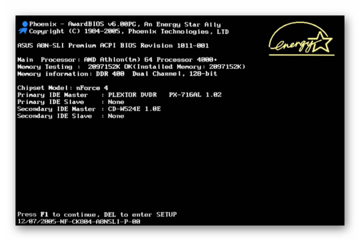
It is quite familiar to many users to hear a beep from the system unit when the computer is turned on. A single short signal indicates that "everything is in order." And if, for example, 1 long signal or a series of sounds sounds instead of it, then it immediately becomes clear that there is a problem. This emits signals to the BIOS, the same program that runs first and tests all components of the computer (from the CPU to the monitor).
The BIOS emits signals during the initial testing of the components of the system unit, while the video card has not yet been initialized, which can display certain text and tabular data on the monitor. With the help of them, you can determine the faulty unit inside the system unit or identify poor contact of external connections.
BIOS errors are encoded into a specific combination of long and short beeps. Moreover, all of them are the same for motherboards of different years of production from almost all manufacturers (from the most famous to "noname"). BIOS audio error codes have a detailed description in the instructions for the motherboard, however, often in English.
The BIOS can make sounds on a mandatory condition: a small, as it is called, system speaker must be connected to the motherboard. Otherwise, BIOS errors will go unnoticed and the user will see only a dark monitor screen.
Sound signals: what is needed to decipher them?
If a single BIOS signal indicates a normal computer startup, then a series of the same short or long sounds (combinations of them) indicates the detection of problems, moreover, of a hardware nature. Then you have to open the cover of the system unit. And even if the user does not interfere with the PC device himself, for example, due to the presence of factory seals on the screws of the cover, decoding these signals will help determine the source of the problem.
Different computer manufacturers may have different beep sounds due to the fact that they use different BIOS versions. Nevertheless, among them you can find those that are typical and most commonly used.
Diagnostics using BIOS sound signals is one of the most effective methods, without the use of special test boards (such as POST-card), therefore, despite the systematic development of production technologies, all motherboards come with a small speaker or, at least, with a connector for its connections.

Sound signals are emitted in the presence of a working power supply and speaker. If they are faulty, then no diagnostics will work. A speaker malfunction can only be determined by replacing it with a known-good copy, which is not always available.
When everything works as intended, then in order to decrypt error codes, you should use a special list that indicates the typical signals for this BIOS version.
Award BIOS beep codes
The most common among the numerous BIOS versions are the versions from the Award developer, who has been making his programs for motherboards since the days when the Pentium trademark did not even exist.
The list of typical signals that are the same for all versions of the Award BIOS is as follows:
- Continuous signal. Breakdown in the power supply. The easiest way to check if this is the case is by replacing the power supply with a known-good copy.
- 2 short. The BIOS pays attention to minor errors, which, nevertheless, require the correct parameters to be entered, for example, by loading the standard factory settings.
- 3 long. The problem is in the keyboard block on the motherboard. The cause can be either a short circuit in the keyboard or connecting cable, or in the motherboard (connector, electronics, electrically conductive dust, etc.).
- 1 long, 1 short. BIOS errors cause RAM modules. The easiest way to fix the problem is to pull out the modules, blow out the accumulated dust from the connector, clean the contacts on the modules themselves and insert them back into the connector. You can leave only one module for the test period and, if necessary, change them, determining which one causes sound signals.
- 1 long, 2 short. . For some models of video cards, such codes are issued when there is poor contact in the monitor connector, when at the moment the BIOS is turned on it cannot determine whether there is a connection with it. To fix the problem, you can do with the video card in the same way as with the RAM in the previous paragraph.
- 1 long, 3 short. The BIOS was unable to initialize the keyboard, which may indicate a malfunction of the keyboard itself, as well as the connector or electronics of the motherboard. The easiest way is to temporarily disable the keyboard, then it will immediately become clear whether it is the source of the problem.
- 1 long, 9 short. Malfunction of the BIOS chip itself. You should just turn off the computer for a while and try turning it on again. If the situation persists and the BIOS error codes do not change, then you should replace the motherboard or try to flash the chip using a special programmer.
- 1 long, constantly repeating. Error initializing memory. It is necessary to replace the modules or at least clean the contacts in the connector and try again.
- 1 short, constantly repeating. Incorrect operation of the power supply. In any case, only a replacement with a serviceable unit or repair of an existing unit will help. Bad contacts are almost never found here due to the large connectors compared to other components of the system unit.
AMI BIOS beep codes
The AMI developer is less common in the BIOS of motherboards than its competitor Award, but, nevertheless, he has firmly occupied his own, albeit small, niche in this market, so you should be ready to meet with his audio signal encoding system.
Deciphering the encoding of audio signals:
- 2 short. The error is caused by incorrect operation of the RAM. In any case, you should start by cleaning the connectors from dust, even if you plan to immediately install new modules to replace the "suspicious" ones.
- 3 short. Like the previous paragraph, indicates a malfunction of the RAM module.
- 4 short. The system timer, which is the basis for the operation of all other components of the motherboard, is faulty. The only thing that can be done without replacing it is to turn off the system unit for a while.
- 5 short. An error occurred while initializing the CPU. You can either turn off the system unit for a while, or remove the cooling system from the processor, pull it out of the socket, and then insert it back. If nothing helps, then you have to change the processor.
- 6 short. The keyboard or its processing unit on the motherboard is faulty. To clarify the source, you can temporarily disable the keyboard, replace it with a known-good copy.
- 7 short. Fault in the motherboard. In such a situation, a careful external examination of the board for the presence of contact-closing debris can help.
- 8 short. Bad video card. You should replace it or, in extreme cases, clean the contacts in the connector. You can temporarily enable the built-in video card and check the operation of the computer with it (if, of course, it is available).
- 1 long, 2 short. Error while initializing video card. The elimination methods are the same as in the previous paragraph.
- 1 long, 3 short. Fault in the video card.
- 1 long, 8 short. The problem is either in the video card or in the monitor.
The following lists of BIOS signals are the basis for diagnosing a computer when there are no other options. In most cases, they allow you to determine the source of the problem, which can simply be replaced with a known-good unit.
If you heard 3 short beeps during the BIOS equipment check procedure, this means that far from everything is in order in your computer. However, it will be difficult for you to find the cause of the malfunction until you look in the BIOS signal table and find out what this signal means.
As you know, different BIOS manufacturers use different tables of sound error messages, and they do not always coincide with each other. As for the situation when you hear 3 short beeps when loading the BIOS, it appears only in some versions of the BIOS.
One such BIOS version is the AMI BIOS. As a rule, if your computer's motherboard is equipped with a similar version of the BIOS, then an informational message containing three short beeps means an error when checking the first 64 KB of RAM.
At present, when the amount of RAM in modern computers is measured in gigabytes, not kilobytes, the chance of receiving such an informational message is small. However, it may appear on some older computers. If such an error still occurs, then you should try to restart the computer using the Reset button. If three short beeps still remain, then you should try to check the reliability of fastening the memory modules in the slots. In the same case, if all the above measures did not bring results, then it will be necessary to change the memory modules.
This signal has a slightly different meaning - three short beeps, it has in the BIOS from AST. In this BIOS, a similar sequence of sounds means something else - a malfunction of the keyboard controller.
If you hear three short beeps when checking the hardware carried out by AST BIOS, then you should not immediately panic. It is possible that after you reboot again, these signals will disappear and you will be able to use the computer again. If this operation did not help restore the computer to working capacity, then you will most likely have to change the keyboard controller, or even the motherboard itself.
Today we will talk about the situation when the computer, when turned on, emits 1 long signal, possibly after a while, a repeating signal and at the same time does not display anything on the screen.
In this situation, there are definitely problems with the equipment. Depending on the motherboard model and BIOS manufacturer, 1 long beep can mean various problems.
Phoenix BIOS thus notifies the user of a fan failure in the CPU cooler. In the Award BIOS, such a combination indicates problems with the power supply. And for the Compaq BIOS, this means a violation of the correct functioning of the RAM.
The IBM BIOS notifies you of video problems with one continuous beep. In some cases, the user can fix such a breakdown on their own. You just need to check how correctly the video card is in the motherboard slot. Perhaps the device should be tweaked a little, and the annoying signal will disappear.
AST BIOS in this case indicates a microcontroller failure. To be more precise, the signal indicates an error detected at the time of checking the first DMA channel. Often, to correct this situation, the user has to change the entire motherboard.
Solutions
So, the first thing to solve this problem is to try to get and install the RAM in place, after wiping its contacts with an eraser. Ideally, take another known working memory and insert it instead of your own.
One of the possible reasons for this sequence of signals is RAM
If after that the problem has not gone away, check if the processor fan is connected to the motherboard properly and if it is not jammed. To do this, try to scroll it with your finger. The computer must be powered off.

Checking the correct connection of the processor cooler
The next step in eliminating one long BIOS signal is to install a known working power supply, which you can temporarily borrow from friends or acquaintances.
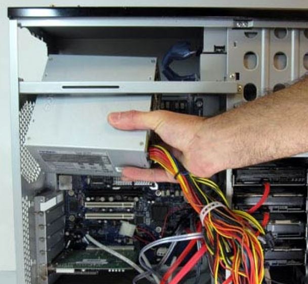
The power supply is one of the possible causes of 1 long BIOS signal
The last step in an attempt to eliminate the prolonged BIOS signal at boot is to try to remove / install the video card by rubbing the contacts with an eraser.

Installing / removing a video card to solve the problem of one short and two long BIOS signals when the computer is turned on
If, after all the steps described, you were unable to start the computer, then most likely you will have to change the entire motherboard.
American Megatrends Inc. (AMI)
The checkpoints of the POST procedures performed in AMIBIOS were revised and supplemented in 1995 and have not undergone significant changes to date. The first description of POST codes or as AMI calls them - "check points" in their current form appeared in connection with the release of the V6.24 kernel, 15/07/95. Some changes have been made in AMIBIOS V7.0 and are reflected in this document.
Features of AMIBIOS startup procedures execution
If during the start process data 55h, AAh appears in the diagnostic port, this information should not be compared with POST codes - we are dealing with a typical test sequence, the task of which is to check the integrity of the data bus.
At the start stage, the data output to the diagnostic port is specific to each platform. In some implementations, the first rendered code is associated with actions, which AMI calls chipset specific stuff. This procedure is accompanied by the output of the CCh value to port 80h and the performance of a number of actions to configure the system logic registers. As a rule, the CCh code occurs in those cases when the system logic from Intel is used, built on the basis of the PIIX controller - these are TX, LX, BX chipsets.
Some onboard I/O chips contain an RTC and a keyboard controller that are in a disabled state upon startup. The purpose of the BIOS is to initialize these board resources for future use. In this case, the first start procedure related to setting up the keyboard controller is accompanied by the output of the value 10h, then the RTC is initialized, as evidenced by the appearance of the DDh code in the diagnostic port. It should be noted that the failure of at least one of these resources will cause the system board as a whole to not start at the very first stage of the POST execution.
On some boards, the initialization process starts with putting the CPU into protected mode. In this case, following the first rendered code 43h, the POST execution continues as described in the AMIBIOS documentation - control is transferred to the D0h point.
Unpackaged initialization codes
Uncompressed Init Code Check Points
| Error code | Error Description |
|---|---|
| EE | In modern implementations of AMIBIOS, the first rendered code is associated with accessing a device from which it is possible to boot to restore the BIOS. |
| CC | System logic register initialization CD Flash ROM type not recognized |
| CE | Checksum mismatch in CF startup BIOS Error accessing spare Flash ROM chip |
| DD | Early initialization of the RTC, which is integrated into the SIO chip |
| D0 | Disable NMI. Development of a time delay for attenuation of transient processes. Boot Block checksum check, stop on mismatch |
| D1 | Perform memory regeneration and Basic Assurance Test. Switching to 4 GB memory address mode |
| D3 | Sizing and Primary Memory Test |
| D4 | Return to real memory addressing mode. Early initialization of the chip set. Installing the stack |
| D5 | Transferring the POST module from Flash ROM to the transit memory area |
| D6 | If the checksum or CTRL + Home does not match, the transition to the Flash ROM recovery procedure is performed (Code E0) |
| D7 | Transferring control to a utility program that unpacks the system BIOS |
| D8 | Complete unpacking of the system BIOS |
| D9 | Transferring control to the system BIOS in Shadow RAM |
| DA | Reading information from SPD (Serial Presence Detect) DIMM DB modules Setting CPU MTRR registers |
| DC | The memory controller is programmed according to the data received from the SPD DE System memory configuration error. Fatal error |
| D.F. | System memory configuration error. Beep 10 Early |
| 11 | Return from STR (Suspend to RAM) state |
| 12 | Restoring access to SMRAM (System Management RAM) |
| 13 | Memory regeneration recovery |
| 14 | Finding and Initializing the VGA BIOS |
Flash ROM Overwriting Procedure Codes
Boot Block Recovery Codes
| Error code | Error Description |
|---|---|
| E0 | Preparations are being made for the interception of INT19 and the possibility of starting the system in a simplified mode is being checked |
| E1 | Setting Interrupt Vectors |
| E3 | CMOS content recovery, BIOS search and initialization |
| E2 | Preparing Interrupt Controllers and Direct Memory Access |
| E6 | Enable interrupts from the system timer and FDC |
| EU | Reinitializing IRQ and DMA ED controllers Initializing the drive |
| EE | Reading boot sector from floppy disk EF Disk operations error |
| F0 | Search for AMIBOOT.ROM file |
| F1 | AMIBOOT.ROM file not found in root directory F2 Read FAT |
| F3 | Reading AMIBOOT.ROM |
| F4 | AMIBOOT.ROM file size does not match Flash ROM size |
| F5 | Disable Internal Cache |
| Determining the type of Flash ROM | |
| FC | Erasing the Main Unit Flash ROM |
| FD | Flash ROM Main Unit Programming |
| FF | BIOS restart |
Unpacked system BIOS codes running in ShadowRAM
Runtime code is uncompressed in F000 shadow RAM
| Error code | Error Description |
|---|---|
| 03 | Disable NMI. Reset Type Definition |
| 05 | Stack initialization. Disable Memory and USB Controller Caching |
| 06 | Executing a utility program in RAM |
| 07 | Processor recognition and APIC initialization |
| 08 | CMOS Checksum Verification |
| 09 | Checking the execution of the End / Ins keys |
| 0A | Battery failure test |
| 0B | Clearing Keyboard Controller Buffer Registers |
| 0C | A test command is sent to the keyboard controller |
| 0E | Finding additional devices served by the keyboard controller |
| 0F | Keyboard initialization |
| 10 | The reset command is sent to the keyboard |
| 11 | If the End or Ins key is pressed, the CMOS is reset. 12 Putting the DMA controllers inactive |
| 13 | Chip set initialization and L2 cache |
| 14 | Checking the system timer |
| 19 | DRAM refresh request generation test in progress |
| 1A | Checking the duration of the regeneration cycle |
| 20 | Initializing output devices |
| 23 | The input port of the keyboard controller is being read. Polling Keylock Switch and Manufacture Test Switch |
| 24 | Preparing to Initialize the Interrupt Vector Table |
| 25 | Interrupt vector initialization complete |
| 26 | The status of the Turbo Switch jumper is polled through the input port of the keyboard controller. |
| 27 | Initialization of the USB controller. Starter microcode update |
| 28 | Preparing to set the video mode |
| 29 | LCD panel initialization |
| 2A | Search for devices served by additional ROMs |
| 2B | VGA BIOS initialization, checking its checksum |
| 2C | Executing VGA BIOS |
| 2D | Matching INT 10h and INT 42h |
| 2E | Search for CGA video adapters |
| 2F | CGA video memory test |
| 30 | CGA Scanner Test |
| 31 | Error in video memory or scanning circuits. Finding an alternative CGA video adapter |
| 32 | Alternative CGA video memory test and scan circuits |
| 33 | Mono/Color Jumper Status Poll |
| 34 | Setting the text mode 80x25 |
| 37 | Video mode is set. Screen cleared |
| 38 | Onboard device initialization |
| 39 | Displaying error messages from the previous step |
| 3A | Display "Hit DEL" message to enter CMOS Setup |
| 3B | Start preparing for a memory test in protected mode |
| 40 | Preparing GDT and IDT Descriptor Tables |
| 42 | Switching to Protected Mode |
| 43 | The processor is in protected mode. Interrupts are allowed |
| 44 | Preparing to test line A20 |
| 45 | Line test A20 |
| 46 | RAM sizing completed |
| 47 | Test data written to Conventional Memory |
| 48 | Rechecking Conventional Memory |
| 49 | Extended Memory Test |
| 4B | Zeroing the memory |
| 4C | Zeroing progress indication |
| 4D | Write to CMOS received sizes Conventional and Extended memory 4E Indication of the actual amount of system memory |
| 4F | Extended Conventional Memory test in progress |
| 50 | Conventional Memory Size Correction |
| 51 | Extended Memory Test |
| 52 | Conventional Memory and Extended Memory volumes preserved |
| 53 | Delayed Parity Error Handling |
| 54 | Disable Parity and NMI Handling |
| 57 | Memory region initialization for POST Memory Manager |
| 58 | You are prompted to enter CMOS Setup |
| 59 | Returning the processor to real mode |
| 60 | Checking DMA page registers |
| 62 | DMA#1 controller address and transfer length register test |
| 63 | DMA#2 Controller Transfer Length and Address Register Test |
| 65 | Programming DMA Controllers |
| 66 | Clearing the Write Request and Mask Set POST Registers |
| 67 | Programming Interrupt Controllers |
| 7F | Allow NMI query from additional sources |
| 80 | Set the interrupt service mode from the PS / 2 port |
| 81 | Keyboard Interface Test on Reset Errors |
| 82 | Setting the Keyboard Controller Mode |
| 83 | Keylock status check |
| 84 | Memory Verification |
| 85 | Displaying error messages |
| 86 | Setting up the system for Setup |
| 87 | Unpacking the CMOS Setup program into Conventional Memory. |
| 88 | Setup program terminated by user |
| 89 | Finished restoring state after Setup |
| 8B | Reserving Memory to an Additional BIOS Variable Block |
| 8C | Configuration register programming |
| 8D | Initialization of HDD and FDD controllers |
| 8F | Reinitializing the FDD Controller |
| 91 | Configuring the hard drive controller |
| 95 | Running a ROM Scan to find additional BIOSes |
| 96 | Additional configuration of system resources |
| 97 | Additional BIOS Signature and Checksum Verification |
| 98 | Configuring System Management RAM |
| 99 | Setting the Timer Counter and Parallel Port Variables 9A Listing the Serial Ports |
| 9B | Preparing an area in memory for a coprocessor test |
| 9C | Coprocessor initialization |
| 9D | Coprocessor information is stored in CMOS RAM |
| 9E | Keyboard Type Identification |
| 9F | Search for additional input devices |
| A0 | Formation of registers MTRR (Memory Type Range Registers) |
| A2 | Error messages on previous initialization steps |
| A3 | Keyboard auto-repeat timing setting |
| A4 | Defragment unused RAM regions |
| A5 | Setting the video mode |
| A6 | Screen cleaning |
| A7 | Migrating BIOS Executable Code Shadow RAM Area |
| A8 | Additional BIOS initialization in segment E000h |
| A9 | Return control to system BIOS AA USB bus initialization |
| AB | Preparing the INT13 module for servicing disk services |
| AC | Building AIOPIC tables to support multiprocessor AD systems Preparing the INT10 module for servicing video services |
| AE | DMI initialization |
| B0 | System configuration table output B1 ACPI BIOS initialization |
| 00 | Software Interrupt INT19h - Loading the Boot Sector |
Features of running Device Initialization Manager
In addition to the above POST codes, event messages are output to the diagnostic port during the execution of the Device Initialization Manager (DIM). There are several breakpoints that display the initialization status of system or local buses.
The information is displayed in word format, the low byte of which matches the system POST code, and the high byte indicates the type of initialization procedure being performed. The high order tetrad in the high byte indicates the type of procedure to be executed, and the low order specifies the bus topology for its application.
Senior tetrad
Junior tetrad
If a system memory configuration error is detected, the DE code, the DF code, the configuration error code, which can take the following values, is output to port 80h sequentially in an endless loop:
2. Award BIOS V4.51PG Elite
AwardBIOS V4.51PG Elite
The dynamically developing company Award Software in 1995 offered a new at that time solution in the field of low-level software - AwardBIOS "Elite", better known as V4.50PG. The checkpoint service mode has not changed in either the widespread version V4.51 or the rare version V4.60. The suffixes P and G denote, respectively, the support of the PnP mechanism and the maintenance of power saving functions (Green Function).
POSTing to Shadow RAM
| Error code | Error Description |
|---|---|
| 03 | Disable NMI, PIE (Periodic Interrupt Enable), AIE (Alarm Interrupt Enable), UIE (Update Interrupt Enable). SQWV Programmable Frequency Generation Prohibition |
| 04 | Checking the formation of requests for regeneration of DRAM |
| 05 | |
| 06 | Test of memory area starting at address F000h where BIOS is located 07 Test of CMOS and battery operation |
| BE | Programming the configuration registers of the South and North Bridges |
| 09 | Initializing L2 Cache and Cyrix Advanced Cache Control Registers |
| 0A | Interrupt vector table generation. Configuring Power Management Resources and Installing the SMI Vector |
| 0B | CMOS checksum check. Scanning the bus PCI devices. Processor microcode update |
| 0C | Keyboard controller initialization |
| 0D | Search and initialization of the video adapter. IOAPIC setting. Clock measurements, FSB setting |
| 0E | MPC initialization. Video memory test. Display Award Logo |
| 0F | Testing the first DMA 8237 controller. Keypad detection and internal test. BIOS checksum check |
| 10 | Checking the second DMA 8237 controller |
| 11 | Checking the page registers of DMA controllers |
| 14 | System Timer Channel 2 Test 15 Request Masking Register Test 1st Interrupt Controller |
| 16 | 2nd interrupt controller request masking register test 19 NMI request passivity check |
| 30 | Determining the amount of Base Memory and Extended Memory. API setup. Programmatic control of the Write Allocation mode |
| Error code | Error Description |
|---|---|
| 31 | The main on-screen test of RAM. USB initialization |
| 32 | The Plug and Play BIOS Extension splash screen is displayed. Setting up Super I/O resources. Programmable Onboard Audio Device |
| 39 | Clock generator programming via I2C bus |
| 3C | Setting the software flag to allow entry in Setup |
| 3D | PS/2 mouse initialization |
| 3E | Initializing the External Cache controller and enabling Cache BF Setting the configuration registers of the chip set |
| 41 | Initializing the floppy disk subsystem |
| 42 | Disable IRQ12 if no PS/2 mouse is present. Hard disk controller soft reset in progress. Scanning other IDE devices |
| 43 | |
| 45 | FPU coprocessor initialization |
| 4E | Error message indication |
| 4F | Password request |
| 50 | Restoring a previously saved CMOS state in RAM |
| 51 | Allow 32 bit HDD access. Configuring ISA/PnP Resources |
| 52 | Initialization of additional BIOS. Setting the values of the PIIX configuration registers. Formation of NMI and SMI |
| 53 | |
| 60 | Installing anti-virus protection BOOT Sector |
| 61 | Final steps to initialize the chip set |
| 62 | Read keyboard ID. Setting its parameters |
| 63 | Correction of ESCD, DMI blocks. Clearing RAM |
| FF | Transferring control to the bootloader. BIOS executes INT 19h |
3. Award BIOS V6.0 Medallion
AwardBIOS V6.0 Medallion
The first mention of the Award Medallion BIOS, Version 6.0 dates back to May 12, 1999. The structure of the new product remained unchanged, retaining the early (Early), late (Late), and final (System) phases of hardware initialization. Significant changes have affected the algorithms for performing POST, which is reflected in the new encoding of checkpoints, significantly expanding their scope. However, the new BIOS did not have a place for outdated technologies such as EISA, and for this reason a number of POST codes were abolished.
Executing POST start routines from ROM
At the stage of early initialization, the BIOS program code is executed from the boot block (Boot Block) in Flash ROM, and is accompanied by the output of checkpoints 91h…FFh to the diagnostic port
| Error code | Error Description |
|---|---|
| 91 | Selecting the CF Platform Start Scenario Determining the Processor Type |
| C0 | Disable External Cache. Disable Internal Cache. Shadow RAM ban. Programming the DMA controller, interrupt controller, timer, RTC C1 block Determining the type of memory, total size and placement in lines 0С Checking checksums |
| C3 | Verification of the first 256K DRAM for the organization of the Temporary Area. Unpacking BIOS in Temporary Area |
| C5 | If the checksums match, the executed POST code is transferred to Shadow. Otherwise, control is transferred to the BIOS recovery procedure. |
| B0 | North Bridge initialization |
| A0-AF | Device-dependent system logic initialization procedure E0-EF Error during system logic initialization process |
BIOS recovery
POSTing to Shadow RAM
Late initialization is performed in RAM and continues until the user menu is called - CMOS Setup. This POST phase is characterized by the use of the E000h memory segment, in which the passage of checkpoints from 01h to 7Fh is processed.
| Error code | Error Description |
|---|---|
| 01 | Unpacking XGROUP at physical address 1000:0000h |
| 03 | Early |
| 05 | Setting the initial values of the variables that define the attributes of the image. Checking the CMOS Status Flag |
| 07 | Checking and initializing the keyboard controller |
| 08 | Determining the interface type of a connected keyboard |
| 0A | Keyboard and mouse auto-detection procedure. Final Keyboard Controller Settings Using PCI Space Registers |
| 0E | Memory segment test F000h |
| 10 | Installed FlashROM Type Definitions |
| 12 | CMOS test |
| 14 | Chipset register initialization procedure |
| 16 | Primary initialization of the onboard frequency synthesizer |
| 18 | Definitions of installed processor and its size Cache L1 and L2 1B Generation of interrupt vector table |
| 1C | |
| 1D | Initial setup of the Power Management system |
| 1F | Loading from external module XGROUP keyboard matrix |
| 21 | Initializing the Hardware Power Management Subsystem |
| 23 | Coprocessor testing. Determining the type of FDD drive. Preparatory step for creating a resource map of PnP devices |
| 24 | Processor microcode update procedure. Resource Allocation Map Update |
| 25 | Initialization and scanning of the PCI bus |
| 26 | Setting up the logic serving the VID (Voltage Identification Device) lines. Initialization of the onboard voltage and temperature monitoring system |
| 27 | Reinitializing the Keyboard Controller |
| 29 | Initialization of the APIC, which is part of the central processor. Measuring the frequency at which the processor operates. Setting up system logic registers. Initializing the IDE Controller |
| 2A | |
| 2B | Search VGA BIOS |
| 2D | Displaying information about the processor |
| 33 | Performing a Reset on a Connected Keyboard |
| 35 | Checking the first channel of the DMA 8237 controller |
| 37 | Checking the second channel of the DMA 8237 controller |
| 39 | Testing DMA page registers |
| 3C | Configuring the Programmable Interval Timer Controller (8254) |
| 3E | Initializing the Master Controller 8259 |
| 40 | Initialization of the Slave controller 8259 |
| 43 | Preparing the interrupt controller for work. Interrupts are disabled, they are enabled later, after a memory test |
| 45 | Non-Maskable Interrupt (NMI) Request Passivity Check |
| 47 | Performing ISA/EISA tests |
| 49 | Determining the amount of basic and extended memory. Software Control of Writes Allocation Mode by Tweaking AMD K5 Registers |
| 4E | Memory testing within the first megabyte and visualization of the results on the display screen. Initialization of caching schemes for single and multiprocessor systems, setting Cyrix M1 processor registers |
| 50 | USB initialization |
| 52 | Testing all available system memory, including the region for the built-in video controller (Shared Memory). Visualization of results on the display screen |
| 53 | Reset your login password |
| 55 | Visualization of the number of detected processors |
| 57 | Initial initialization of ISA PnP devices, each of which is assigned a CSN (Card Select Number). Visualization of the EPA logo |
| 59 | Initialization of the anti-virus support system |
| 5B | Starting the BIOS update procedure from the 5D floppy drive Initializing the on-board SIO and Audio controllers |
| 60 | Access to CMOS Setup is open |
| 63 | PS/2 Mouse initialization |
| 65 | USB Mouse initialization |
| 67 | Use of IRQ12 by PCI Devices if PS/2 Mouse System Doesn't Have 69 Full L2 Cache Controller Initialization |
| 6B | Chipset initialization according to CMOS Setup |
| 6D | Configuring resources for ISA PnP devices in SIO 6F configuration mode Initializing the floppy disk subsystem |
| 73 | Preliminary steps to initialize the hard drive subsystem. On some platforms - ALT+F2 poll to launch AwardFlash |
| 75 | Finding and initializing IDE devices |
| 77 | Initializing Serial and Parallel Ports |
| 7A | Software reset of the coprocessor, writing the control word to the register FPU CW 7C Setting the protection against unauthorized writing to hard disks |
| 7F | Output of error messages. Maintaining the DEL and F1 keys |
Preparing tables, arrays and structures to start the operating system
Starting with code 82h, POST configures the system according to the CMOS settings. Its final phase is executed from the Shadow RAM area (segment E800h) and ends with the transfer of control to the operating system - code FFh.
| Error code | Error Description |
|---|---|
| 82 | Allocate an area in system memory for power management |
| 83 | Restoring data from the temporary storage stack in CMOS |
| 84 | Displaying the message "Initializing Plug and Play Cards..." |
| 85 | USB initialization completed |
| 86 | Reserved, clearing Carry Flag |
| 87 | Building SYSID tables in the DMI area |
| 88 | Reserved, clearing Carry Flag |
| 89 | Generating ACPI Maintenance Tables |
| 8A | Reserved, clearing Carry Flag |
| 8B | Finding and initializing the BIOS of additional devices |
| 8C | Reserved, clearing Carry Flag |
| 8D | Initialization of parity bit maintenance routines |
| 8E | Reserved, clearing Carry Flag |
| 8F | IRQ12 resolution for mouse hot plugging 90 Reserved, Clear Carry Flag |
| 91 | Initializing Legacy Platform Resources |
| 92 | Reserved, clearing Carry Flag |
| 93 | Presumably not used |
| 94 | Final steps to initialize the main set of logic before loading the operating system. Power management system initialization completes. The BIOS startup screen saver is removed, the resource allocation table is displayed on the screen. For AMD K6® family processors, specific settings are made. Firmware Update for Intel Pentium® II Processor Family and Above |
| 95 | Sets the automatic changeover mode for winter/summer time. Programming the Keyboard Controller for an Auto-Repeat Rate |
| 96 | In multiprocessor systems, final system settings are performed and service tables and fields are created. For processors of the Cyrix family, additional register tuning is performed. Building the ESCD table "Extended System Configuration Data". Set DOS Time counter according to Real Time Clock. Partitions of boot devices are saved for further use by built-in anti-virus tools: Trend AntiVirus or Paragon Anti-Virus Protection. The system speaker signals the end of the POST execution. The MSIRQ table is built and saved |
A number of processes that take place in the Award Medallion BIOS are identified by special checkpoint groups. These include:
System Event codes - control points of system events.
Power Management Debug codes - checkpoints that occur during the execution of APM or ACPI services.
System Error codes - fatal error messages.
Debug codes for MP system - initialization points for multiprocessor platforms.
POST Fast Track Features
The user can select the "Quick Power On Self Test" option in CMOS Setup to reduce system boot time. In this case, the passage of POST will be accelerated by refusing to perform some procedures (Quick Boot).
The Quick Boot scheme replaces the late and final POST phases and does not affect the operation of the boot block. Award Software offers a non-standard codification of the executable POST fast-track procedures. Quick Boot starts with checkpoint 65h output to the diagnostic port and ends with POST code 80h. Control is then transferred to the operating system, displaying the usual Award BIOS code FFh.
| Error code | Error Description |
|---|---|
| 65 | Early initialization of the SIO controller, software reset of the video controller. Keyboard controller setup, keyboard and mouse test. Sound controller initialization. Checking the integrity of BIOS structures. Unpacking the Flash ROM Maintenance Procedures. Initialization of the onboard frequency synthesizer |
| 66 | Initialize the L1/L2 cache according to the results obtained from the CPUID command. Generation of a vector table consisting of pointers to interrupt routines. Initializing Power Management Hardware |
| 67 | CMOS and battery validation. Setting the chipset registers according to the CMOS settings. Initialization of the keyboard controller in the chipset. Generating BIOS Data Area Variables |
| 68 | Video system initialization |
| 69 | Configuring the i8259 Interrupt Controller |
| 6A | An accelerated one-pass test of RAM is performed using a special algorithm |
| 6B | Visualization of the number of detected processors, the EPA logo, and an invitation to launch the AwardFlash utility. Configuring Embedded I/O Controller Resources in Configuration Mode |
| 70 | Setup prompts. Initializing PS/2 and USB Mouse |
| 71 | Cache Controller Initialization |
| 72 | Setting configuration registers for system logic. Formation of the list of Plug and Play devices. FDD controller initialization |
| 73 | HDD controller initialization |
| 74 | Coprocessor initialization |
| 75 | If specified by the user in the CMOS Setup, the IDE HDD is write-protected |
| 77 | Password prompt and message: "Press F1 to continue, DEL to enter Setup" |
| 78 | BIOS initialization of additional devices on ISA and PCI buses |
| 79 | Initializing Legacy Platform Resources |
| 7A | Generation of RSDT root table and device tables DSDT, FADT, etc. |
| 7D | Finding Information About Boot Device Partitions |
| 7E | Configuring BIOS Services and Services Before Booting the Operating System |
| 7F | Setting the NumLock flag according to CMOS SetUp |
| 80 | Transfer control to the operating system |
Performing POST in Power Saving Mode
One of the platform states, when the contents of RAM is stored on the hard disk, is called Hibernate. In the ACPI specification ("Advanced Configuration and Power Interface Specification", Revision 2.0a dated 03/31/2002), it is defined as S4 (Non-Volatile Sleep) power saving mode. Returning to full functionality involves a special way of passing the POST.
The ACPI S4 operation scheme, as in the case of an accelerated start, replaces the late and final POST phases. An essential point is the check in the boot block of the start script. Depending on the ACPI state the system is in after the hardware Reset signal, a decision is made to exit the S4 state, which begins with the output of the 90h checkpoint to the diagnostic port and ends with the POST code 9Fh.
| Error code | Error Description |
|---|---|
| 90 | Early initialization of the SIO controller, software reset of the video controller. Keyboard controller setup, keyboard and mouse test |
| 91 | CMOS and Battery Validation |
| 92 | Initialization of system logic registers and on-board frequency synthesizer |
| 93 | Cache Initialization Based on CPUID Information |
| 94 | Generation of a vector table consisting of pointers to interrupt routines. Initializing Power Management Hardware |
| 95 | PCI bus scan |
| 96 | Initializing the built-in keyboard controller |
| 97 | Video system initialization |
| 98 | Displaying VGA adapter messages |
| 99 | Checking the first channel of the DMA8237 controller by writing and checking the reading of the registers of the base address and the length of the transfer block 9A Configuring the i8259 interrupt controller |
| 9B | PS/2 and USB Mouse initialization. Unpacking ACPI code. Cache controller initialization |
| 9C | Setting configuration registers for system logic. Formation of the list of Plug and Play devices. Initialization of FDD and HDD controllers |
| 9D | A PM region reservation in system memory is not performed if one is created in Shadow RAM or SMRAM. In some cases, a final USB bus initialization is required, performed with the L1 cache disabled |
| 9E | Setting up Power Management, which is part of the system logic. Initialize the SMI generation circuits and set up the SMI vector. Programming Resources Responsible for Monitoring PM System Events |
| 9F | The disable/enable operation clears the L1/L2 cache and restores its current size. The power saving control settings specified in CMOS Setup are stored in PM RAM. For mobile platforms, a check is made to return to full operation after turning off all supply voltages (Zero Volt Suspend mode) |
4. Phoenix BIOS 4.0 Release 6.0
Phoenix Technologies Ltd.
Phoenix Technologies, one of the leaders in the development of low-level software, timed the release of Windows95 with a new version of PhoenixBIOS 4.0. Support for the Intel Pentium processor family is reflected in the name of the interim revisions. One of the latest - Release 6.0 - formed the basis of all released BIOSes. Since Release 6.1, there have been no significant changes in the way POSTs are executed, and therefore this has not been reflected in the indication of breakpoints.
A distinctive feature of PhoenixBIOS is that if during the POST execution there are errors in testing 512 KB of main memory (codes 2Ch, 2Eh, 30h), additional information is output to port 80h in the format of a word, the bits of which identify the failed address line or data cell. For example, the code "2C 0002" means that a memory failure has been detected on address line 1. The code "2E 1020" in this case would mean that a failure has been detected on data lines 12 and 5 in the low byte of the memory data bus. On 386SX systems using a 16-bit data bus, an error cannot occur at runtime code 30h.
The output of the POST code to the diagnostic port is accompanied by the output of a sound signal to the system speaker. The scheme for generating an audio signal is as follows:
- Eight-bit code is converted into four two-bit groups
- The value of each group is incremented by one
- Based on the received value, a short beep is generated (for example: code 16h = 00 01 01 10 = 1-2-2-3)
Executing POST start routines from ROM
| Error code | Error Description |
|---|---|
| 01 | Initializing the Baseboard Management Controller (BMC) |
| 02 | Checking the current processor mode |
| 03 | Disable NMIs |
| 04 | Determines the type of processor installed |
| 06 | Initial settings of the PIC and DMA registers |
| 07 | The area in memory intended for the copy of the BIOS is reset to zero |
| 08 | Early initialization of system logic registers |
| 09 | Setting the POST execution software flag |
| 0A | Initialization of software resources of the processor |
| 0B | Permission Internal Cache |
| 0E | Super I/O Resource Initialization |
| 0C | Initialize L1/L2 cache according to CMOS values |
| 0F | IDE initialization |
| 10 | Initializing the Power Management Subsystem |
| 11 | Setting Alternate Register Values |
| 12 | MSW (Machine Status Word) register value is being set |
| 13 | Early initialization of PCI devices |
| 14 | Keyboard controller initialization |
| 16 | Checksum ROM BIOS |
| 17 | L1/L2 Cache Sizing |
| 18 | Initializing the 8254 system timer |
| 1A | DMA controller initialization |
| 1C | Reset programmable interrupt controller values |
| 20 | Checking the Formation of DRAM Refresh Requests |
| 22 | Testing Keyboard Controller Operation |
| 24 | Installing a selector to serve a flat 4Gb memory model |
| 26 | A20 line resolution |
| 28 | Determining the total amount of installed memory |
| 29 | Initializing POST Memory Manager (PMM) |
| 2A | Zeroing 640Kb main memory |
| 2C | Address line testing |
| 2E | Failure on one of the data lines in the low byte of the memory data bus |
| 2F | Selecting a cache protocol |
| 30 | Available system memory test |
| 32 | Determination of CPU clock parameters and bus frequency |
| Error code | Error Description |
|---|---|
| 33 | Phoenix Dispatch Manager initialization |
| 34 | Power Off Prohibition with ATX Power Button |
| 35 | Settings for system logic registers that control the formation of timing characteristics of access to memory, I / O ports, system and local buses |
| 36 | A restart is performed if the transition to the next POST procedure fails. The sequence of procedures is managed by Watch Dog Service |
| 37 | The process of setting up the system logic registers is being completed |
| 38 | The content of the BIOS module Runtime is unpacked and rewritten to the area intended for Shadow RAM |
| 39 | Reinitializing the Cache Controller |
| 3A | Resizing the L2 Cache |
| 3B | Initializing the BIOS Execution Trace |
| 3C | Additional setting of logic registers for configuring PCI-PCI bridges and supporting distributed PCI buses |
| 3D | The system logic registers are configured in accordance with the CMOS Setup settings. |
| 3E | Read Hardware Configuration |
| 3E | Checking the connection of the ROM Pilot system |
| 40 | Determination of the CPU clock parameters |
| 41 | Initializing ROM Pilot - Remote Boot Management |
| 42 | |
| 44 | Set BIOS Interrupt |
| 45 | Device initialization before enabling the PnP mechanism |
| 46 | Using a special algorithm, the BIOS checksum is calculated |
| 47 | Initializing I2O I/O Controllers |
| 48 | Finding a video adapter |
| 49 | PCI Initialization |
| 4A | Initializing system video adapters |
| 4B | Quiet Boot in progress - an abbreviated system startup sequence used to speed up POST |
| 4C | VGA BIOS content is written to pass-through area |
| 4E | BIOS Text String Visualization Copyright |
| 4F | Reserving memory for the boot device selection menu |
| 50 | The type of processor and its clock frequency are visualized |
| 51 | Initializing the Controller and EISA Devices |
| 52 | Keyboard controller programming |
| 54 | Key beep mode activated |
| 55 | |
| 58 | Search for Unhandled Interrupt Requests |
| 59 | POST Display Service (PDS) initialization 5A Message "Press F2 to enter SETUP" output |
| 5B | Disable CPU Internal Cache |
| 5C | Checking Conventional Memory |
| 5E | Detect Base Address |
| 60 | Check Extended Memory |
| 62 | Checking Extended Memory Address Lines |
| 64 | Transfer control to an executable block generated by the motherboard manufacturer (Patch1) |
| 66 | Configuring Cache Control Registers |
| 67 | Minimal initialization of APIC controllers |
| 68 | L1/L2 cache resolution |
| 69 | Preparing System Management Mode RAM |
| 6A | The volume of External Cache is visualized |
| 6B | Setting CMOS Setup Defaults |
| 6C | Visualization of information about the use of Shadow RAM |
| 6E | Visualization of information about Upper Memory Blocks (UMB) |
| 70 | Displaying error messages |
| 72 | Checking the current system configuration and information in CMOS |
| 76 | Checking Keyboard Error Information |
| 7A | Checking the status of software (System Password) or hardware (Key Lock Switch) keyboard locks |
| 7C | Setting hardware interrupt vectors |
| 7D | Power Tracking Initialization |
| 7E | Coprocessor initialization |
| 80 | On-board SIO I/O controller is prohibited |
| 81 | Preparing to boot the operating system |
| 82 | Finding and identifying RS232 ports |
| 83 | Configuring External IDE Controllers |
| 84 | Finding and identifying parallel ports |
| 85 | Initializing ISA PnP Devices |
| 86 | On-board resources of the SIO controller are configured according to the CMOS Setup settings |
| 87 | Configuring MCD (Motherboard Configurable Devices) |
| 88 | The values of the variable block are set in the BIOS Data Area |
| 89 | NMI generation enabled |
| 8A | Setting Variable Values in the Extended BIOS Data Area |
| 8B | Checking PS/2 Mouse Wiring Diagrams |
| 8C | Drive controller initialization |
| 8F | Determining the number of connected ATA devices |
| 90 | Initializing and configuring hard disk controllers |
| 91 | Setting temporary parameters for hard drives in PIO mode |
| 92 | Transfer control to an executable block generated by the motherboard manufacturer (Patch2) |
| 93 | Building a configuration table for a multiprocessor system |
| 95 | Selecting a CD-ROM Maintenance Procedure |
| 96 | Return to Real Mode |
| 97 | Building an MP Configuration Table |
| 98 | ROM Scan in progress |
| 99 | Checking the status of the SMART parameter 9A ROM contents are being written to RAM |
| 9C | Setting up the Power Management subsystem |
| 9D | Initialization of resources for protection against unauthorized access |
| 9E | Enable hardware interrupts |
| 9F | Determines the number of IDE and SCSI drives |
| A0 | Setting DOS Time according to RTC status A1 The purpose of this code is unknown A2 Checking the status of Key Lock |
| A4 | Keyboard auto-repeat characteristic settings |
| A8 | The message "Press F2 to enter Setup" is removed from the screen |
| AA | Checks for the presence of the SCAN key code F2 in the AC input buffer Runs the Setup program |
| AE | CTRL+ALT+DEL restart flag is cleared B0 "Press F1 to resume, F2 to Setup" message is generated |
| B1 | POST complete flag cleared B2 POST completed |
| B4 | Playing a beep before downloading |
| B5 | Quiet Boot phase completed |
| B6 | Password check if this mode is enabled in Setup B7 ACPI BIOS initialization |
| B9 | Search for boot devices on the USB bus BA Initialize DMI parameters |
| BB | Re-executing the ROM Scan procedure |
| BC | The RAM parity error latch trigger is reset to zero. |
| BD | A menu is displayed to select a boot device BE Clearing the screen before loading the operating system BF Activating anti-virus support |
| C0 | The procedure for processing the software interrupt INT 19h is launched - the Boot Sector loader. The interrupt routine attempts to load the Boot Sector sequentially by polling disk devices in the order prescribed by Setup. |
| C1 | Initialization of the fault handling procedure (PEM) C2 Call service procedures for error logging |
| C3 | Visualization of error messages in the order of their arrival C4 Setting flags of initial states |
| C5 | Extended CMOS RAM cell block initialization |
| C6 | Dock Initialization |
| C7 | Delayed Dock Initialization |
| C8 | Execution of test procedures included in the Boot Block to determine the integrity of BIOS structures |
| C9 | Checking the integrity of structures and / or modules external to the system BIOS |
| CA | Running Console Redirect to service a remote CB keyboard Emulating disk devices in RAM/ROM |
| CC | Run Console Redirect to serve video CD Support PCMCIA communication |
| CE | Setting up the light pen controller |
Fatal error messages
D0 Error caused by an exception (Exception error) D2 Calling the interrupt handling procedure from an unidentified source D4 Error related to violation of the protocol for issuing and removing interrupt requests D6 Exit protected mode with software generated reset D7 To save the state of the video adapter, more is required amount of memory than available in SMRAM D8 Error during software generation of processor reset pulse DA Loss of control when returning to Real Mode DC Exit protected mode with software generation of reset without reinitializing the interrupt controller DD Error during extended memory testing DE Keyboard controller error DF Line control error A20 19
Executing Procedures from the Boot Block
| Error code | Error Description |
|---|---|
| E0 | E1 Chipset Configuration Register Setup Northbridge and Southbridge Initialization |
| E2 | CPU initialization |
| E3 | Initializing the system timer |
| E4 | Super I/O Resource Initialization |
| E5 | Checking the Status of the Recovery Jumper, Installing Which Forces the BIOS Recovery Mode |
| E6 | BIOS checksum check |
| E7 | Control is transferred to the BIOS if its checksum is calculated correctly E8 MPS support initialization |
| E9 | Transition to a flat 4Gb memory model |
| EA | Initialization of non-standard equipment |
| EB | Configuring the Interrupt Controller and Direct Memory Access |
| EU | By means of writes and control readings according to a special algorithm, the type of memory is determined: FPM, EDO, SDRAM, according to the result, the Host Bridge configuration registers are configured |
| ED | By means of records and control readings according to a special algorithm, the volume of memory banks and placement by lines are determined. According to the result, the configuration registers of the Host Bridge (DRAM Row Boundary) are configured. |
| EE | The contents of the Boot Block are copied to Shadow RAM EF Preparing SMM RAM for the SMI handler |
| F0 | Memory test |
| F1 | Interrupt vector initialization |
| F2 | Initializing Real Time Clock |
| F3 | Video subsystem initialization |
| F4 | Generating a beep before downloading |
| F5 | Loading an operating system stored in Flash ROM |
| F6 | Return to Real Mode |
| F7 | Boot to Full DOS |
| F8 | USB controller initialization |
| FA…FF | Interaction codes with PhDebug procedure |
5. Inside BIOS Mobile Pro
Inside Software Corp.
The mobile systems market insider has firmly established himself where loyalty to tradition and a conservative approach to building a BIOS are required. Having inherited the source code from SystemSoft, the company is constantly working to improve it. The last of the MobilePRO revisions is actively used in Mitac and Clevo laptops, the documentation for which formed the basis of the Error Codes table - this is how Insyde Software calls POST execution checkpoints.
Boot Block Checkpoints
Despite the fact that Insyde Software created its first BIOS in 1992, the well-established boot block model - or Boot Loader, as the creators themselves called it - was finally formed only by the end of 1995. From that moment on, the starting procedure was numbered according to the version and date of creation.
The most significant point from the point of view of a service engineer investigating the process of booting a computer system with InsydeBIOS is the device for displaying diagnostic codes. Although, as a rule, the Boot Loader uses the Manufacture's Diagnostic Port 80h, which is standard in such cases, in some cases, checkpointing is performed only on the PIO Port (Parallel Input / Output port for diagnostic purpose), which is nothing more than parallel port 378h There are implementations in which diagnostic codes sent to port 80h are duplicated to the parallel port.
| Error code | Error Description |
|---|---|
| 00 | Boot Block Execution Start Point 01 Inhibit Line A20 (Not Used) |
| 02 | CPU microcode update |
| 03 | RAM testing |
| 04 | Moving the boot block to RAM |
| 05 | Execute boot block from RAM |
| 06 | Forcing the Flash ROM Recovery Procedure |
| 07 | Transferring the system BIOS to RAM |
| 08 | System BIOS Checksum Verification |
| 09 | Starting the POST procedure |
| 0A | Starting the Flash ROM recovery procedure from the FDD drive |
| 0B | Frequency synthesizer initialization |
| 0C | Completing the BIOS Recovery Procedure |
| 0D | Alternative Flash ROM recovery procedure with FDD |
| 0F | Stop on fatal error |
| BB | Early initialization of LPC SIO |
| CC | Starting point for flash ROM recovery |
| 88 | Enable ACPI functions |
| 99 | Error exiting STR mode |
| 60 | Entering Big Real Mode |
| 61 | SM Bus initialization. SPD data stored in CMOS A0 Read and parse SPD fields previously stored in CMOS A1 Initialize memory controller |
| A2 | Determining the logical banks of a DIMM |
| A3 | Programming registers DRB (DRAM Row Boundary) |
| A4 | DRA (DRAM Row Attributes) Register Programming |
| AE | The system detected DIMMs that differ in Error Correcting Codes (ECC) functions |
| AF | Primary initialization of memory controller registers mapped in memory space |
| E1 | Boot procedure fails if DIMM does not have an SPD chip |
| E2 | DIMM type does not match system requirements |
| EA | Minimum time between activation of DIMM rows and transition to regeneration state does not meet system requirements |
| EU | Register modules are not supported by ED Checking CAS Latency Modes |
| EE | DIMM organization not supported by motherboard |
Performing POST procedures from RAM
Most modern InsydeBIOS solutions use 16-bit checkpoint mapping. For this, ports 80h and 81h are used, the latter of which is intended to extend the standard diagnostics.
The study of control points is hampered by their irregular construction, when processes that are different in meaning are accompanied by the same codes. In dual diagnostic systems, there are heterogeneities of a different order: some POST codes are displayed only in one of the ports without the usual duplication in such cases.
| Error code | Error Description |
|---|---|
| 10 | Cache initialization, CMOS check |
| 11 | A20 line ban. Setting registers for 8259 controllers. |
| 12 | Determining the download method |
| 13 | Memory controller initialization |
| 14 | Finding a video adapter connected to the ISA bus |
| 15 | Setting System Timer Values |
| 16 | Setting system logic registers via CMOS |
| 17 | Counting the total amount of RAM |
| 18 | Testing the minor page of Conventional Memory |
| 19 | Flash ROM Image Checksum Verification |
| 1A | Resetting the interrupt controller registers |
| 1B | Video adapter initialization |
| 1C | Initialization of a subset of video adapter registers compatible with the 6845 programming model |
| 1D | EGA adapter initialization |
| 1E | CGA adapter initialization |
| 1F | DMA controller page register test |
| 20 | Keyboard controller check |
| 21 | Keyboard controller initialization |
| 22 | Comparison of the received amount of RAM with the value in CMOS |
| 23 | Battery backup and Extended CMOS test |
| 24 | Testing DMA controller registers |
| 25 | Setting DMA controller parameters |
| 26 | Interrupt vector table generation |
| 27 | Accelerated determination of the amount of installed memory |
| 28 | Protected Mode |
| 29 | System memory test completed |
| 2A | Exit Protected Mode |
| 2B | Transferring the Setup Procedure to RAM |
| 2C | Starting the video initialization procedure |
| 2D | Re-search for CGA adapter |
| 2E | Re-search for EGA/VGA adapter |
| 2F | Displaying VGA BIOS Messages |
| 30 | Keyboard controller custom initialization routine |
| 31 | Checking the connected keyboard |
| 32 | Checking the passage of the request from the keyboard |
| 33 | Keyboard status register check |
| 34 | Test and reset system memory |
| 35 | Protected Mode |
| 36 | Extended memory test completed |
| 37 | Exit Protected Mode |
| 38 | A20 line ban |
| 39 | Cache Controller Initialization 3A System Timer Check |
| 3B | Setting the DOS Time counter according to Real Time Clock |
| 3C | Initializing the hardware interrupt table |
| 3D | Search and initialization of manipulators and pointers |
| 3E | Setting the status of the NumLock key |
| 3F | Initializing Serial and Parallel Ports |
| 40 | Configuring Serial and Parallel Ports |
| 41 | FDD controller initialization |
| 42 | HDD controller initialization |
| 43 | USB Power Management initialization |
| 44 | Finding and Initializing Additional BIOSes |
| 45 | Resetting the NumLock Key Status |
| 46 | Checking coprocessor functionality |
| 47 | PCMCIA initialization |
| 48 | Preparing to start the operating system |
| 49 | Transfer control to Bootstrap executable code |
| 50 | ACPI initialization |
| 51 | Initializing Power Management |
| 52 | USB Bus Controller Initialization |


, poultry farming")


- Burns, Robert - short biography
- The concept of common vocabulary and vocabulary of limited use
- Nancy Drew: The Captive Curse Walkthrough Nancy Drew Curse of Blackmoore Manor Walkthrough
- Deadpool - Troubleshooting
- Won't start How to Survive?
- What to do if bioshock infinite won't start
- Walkthrough Nancy Drew: Alibi in Ashes
- Spec Ops: The Line - game review, review Spec ops the line crashes on missions
- Room escape level 1 walkthrough
- Processing tomatoes with boric acid How much will 2 grams of boric acid
- Cucumber Grass (Borago)
- Bioinsecticide Lepidocid: purpose, properties and application procedure Lepidocide waiting period
- How to change the language to Russian in steam
- Dendrobium noble: room care
- Morphology of plants general concepts - document
- Planting, propagation and care of bamboo at home, photo Growing bamboo from seeds
- How to strengthen the cellular signal for the Internet in the country
- Sanskrit reveals the forgotten meaning of Russian words (2 photos)
- The oldest language Sanskrit programming language of the future Dead language Sanskrit
- Who has dominion over all the earth?